What is the Future for THz Electronic and Photonic Circuits?
| December 3, 2012 | Posted by Frank Gomez under COMSOC, EDCAS, MTT/APS |
Comments off
|
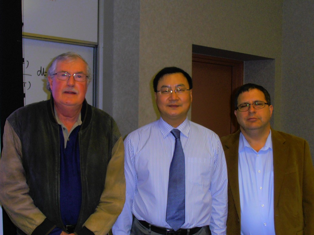
Thursday evening, November 29, 2012, was an opportunity for many RF and Microwave professionals in the LA area to assemble at Cal Tech in Pasadena for an enlightening lecture given by Professor Ke Wu. Professor Wu is from the Ecole Polytechnic Montreal, where he is also actively involved in numerous research efforts in Quebec, Canada. This meeting was jointly sponsored by the IEEE sections in LA, San Fernando Valley, Coastal LA, Orange County and Foothill. All sections had attendees present, as did the Cal Tech staff and their graduate students.
Right from the start, Professor Wu raised the issues of most interest to practicing IEEE engineers: manufacturability, associated process costs, and integration of microwave devices needed to lengthen device working lifespan.
These issues were noted as he made a quick voyage through microwave developments:
First generation: Rigid Waveguides, or how 3–dimensional structures were used to send a 1-dimensional signal;
Second generation: Microwave integrated circuits (MIC) without any active components;
Third generation: Miniature MIC ( MMIC) with the addition of lumped active elements;
Fourth Generation: Multilayered MMIC, and well and MEMS and RFIC devices.
Now, with the arrival and current exploratory development of Substrate Integrated Circuits(SIC), we are starting a new “voyage” of discovery. In short, SIC refers to the technique of using a microstrip line on the top layer, a metalized ground plane, a row of vias or feed-through openings to bound the wave path in the lateral directions, and bonding –dielectric material filling the other spaces. With this configuration, only TEM or TE modes can propagate within the device. (Yes, mode conversions between these two modes can be made at the heterogeneous circuit boundaries.
Some advantages that are undergoing development now include in SICs: use of non-planar substrate for planar modes; complete integration of a planar device; synthesized wave-guides; and many potential hybrid and monolithic features.
As examples of what is happening right now, Professor Wu gave numerous device summaries:
K-band (15 GHz to 35 GHz) receiver filter for SATCOM applications (priced at $700. to $1000. per filter for a relatively small run);
SIC waveguide antennas with large ~60 dB isolation;
SIC directional coupler;
SIC self-oscillating mixer;
And, an integrated FM-CW system-on-substrate.
(Yes, we are talking about laboratory activity around the world. Remember, globalization, everyone.)
Naturally, with this audience and the location at Cal Tech, Professor Wu left us with a list of challenges for future RF developments:
(1) Nano-structures with “near zero loss tangents” and agile, tunable substrates. (We need to reduce power dissipation and increase the life span of active devices.)
(2) Traveling wave E-O (electro-optical)devices
(3) Mixed integration of different wave-guides on a substrate, so as to support multiple modes.
(4) High density multilayer integration.
(5) Monolithic integration of both Active and Passive devices on a substrate, including antennas. Avoid discrete transistors and diodes at high frequencies. (We need to get away from the V /I mode analyses approaches, and think in terms of waves and their associated modes. But, just how???)
(6) Sub-mm Very Large Scale Integration (VLSI)
(7) Explore terahertz electronics (yes, we learn to use plasmon effects) and photonics. Bridge the gap between electronics and photonics. (OK, so we must go back to find “new ” materials.)
After the meeting , our Foothill representatives asked Professor Wu about his views on why we need to explore higher and higher microwave materials, and what direction we should take to make new integrated “microwave transistor-like devices”. His answers, while tentative and speculative, are most interesting. But, we will hold them for a future discussion.

